Switched-Mode Power Supplies
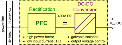
The energy for supplying IT plants of telecom and data centers is drawn in normal mode from the national power grid. The power supply units required for the feeding of a DC voltage bus from a national grid, often referred to as front-end converter, typically consists of a PFC-stage for a non disturbing rectification of the grid voltage, and a DC-DC stage which converts the intermediate voltage at the DC link capacitor to the required output DC voltage while stabilizing it towards fluctuations of the load adjacent to the DC voltage bus (cf. Fig. 1).
In our department we analyze and develop converter stages of high power supply systems in different sub-projects. The actual projects focus on the digital control within a SMPS and the optimization of the LLC resonant converter.
Digital control of switched-mode power supplies
Common power supplies for telecom or server applications are controlled by a cascaded control structure with an outer voltage loop and an inner current loop. Additionally a multitude of protection circuits and monitoring functions are needed. Because of high switching frequencies of some 10 up to some 100 kHz analog circuits are still the preferred choice in order to solve these time critical tasks. Due to advantages such as flexibility and programmability, decreased number of active and passive components, negligible thermal drifts and the possibility of implementing sophisticated adaptive control algorithms, digital control becomes more and more attractive.The aim of different research projects is to realize these control functions within power supplies with micro-controllers or digital signal processors (DSP) [1-3].
In this context, the possibility of implementing adaptive and nonlinear control methods is utilized as well as the development of power management strategies. Such strategies should ensure the maximum efficiency in every operating point while considering the specification, e.g. total harmonic distortion (THD), power factor and hold up behavior. In addition to an improved control performance, also an economic benefit from this process is expected.
Development of power factor correction (PFC) rectifiers for one- and three-phase applications
Passive rectification, which has very poor performance with respect to power factor and THD, are still available in plenty of today's devices. The THD of these devices lead to additional conduction losses and can cause line oscillation. The aim of this research project is to develop and optimize switched-mode power supplies with active PFC rectification. Therefore new topologies and control strategies are investigated to reduce THD as well as weight, volume and costs while at the same time achieving high dynamics, e.g. at load steps [1,3].
Optimization of the LLC resonant converter for the use in high power supplies
The LLC resonant converter is particularly suited in terms of high efficiency to fulfill the DC-DC conversion in a front-end converter. The main reasons lie in the sinusoidal shape of the current and voltage waveforms and the resulting switching conditions for the semi-conductor components (zero voltage/zero current switching), the use of most of the parasitical characteristics of the transformer, as well as the one-stage output filter comprising a single filter capacitance.
The following aspects complicate the use of LLC resonant converters compared to the classical topologies:
- Lots of power supply systems require a controlled limitation of the DC-DC converter output current due to the parallel connection of several front end converters or at overload condition. In case of the LLC converter, the DC-DC gain characteristic arising from the LLC resonant circuit yields the need of additional circuitry to make the output current controllable. This topic is addressed in [4].
- The LLC resonant circuit consists of reactive components which can be manufactured only with moderate allowance. Furthermore, their values change because of aging, especially with respect to the resonant capacitor. These tolerances make an optimal converter design more complicated.
- An optimal design of the LLC converter requires additional iteration steps because of the higher circuit complexity and the above mentioned influence of parameter variations within the resonant circuit elements. This is also new to engineers who are used to classical topologies.
Considering all these aspects, methods especially for the optimal design of the LLC converter are developed in our department, whereby CAE tools written in e.g. Matlab, Mathematica or Mathcad are used.
References:
| [1] | T. Grote, F. Schafmeister, H. Figge, N. Fröhleke, J. Böcker Digital Control Strategy for Multi-Phase Interleaved Boundary Mode and DCM Boost PFC Converters IEEE Energy Conversion Congress and Exposition (ECCE2011), Phoenix, Arizona, USA, 2011 |
| [2] | T. Grote, F. Schafmeister, H. Figge, N. Fröhleke, P. Ide, J. Böcker Adaptive Digital Slope Compensation for Peak Current Mode Control 1st IEEE Energy Conversion Congress and Exposition (ECCE2009), San Jose, California, USA, 2009 |
| [3] | T. Grote, H. Figge, N. Fröhleke, W. Beulen, F. Schafmeister, P. Ide, J. Böcker Semi-Digital Interleaved PFC Control with Optimized Light Load Efficiency Applied Power Electronics Conference and Exposition (APEC), Twenty-Fourth Annual IEEE, Washington DC, USA, 2009 |
| [4] | H. Figge, T. Grote, N. Fröhleke, J. Böcker, F. Schafmeister Overcurrent Protection for the LLC Resonant Converter with Improved Hold-Up Time Applied Power Electronics Conference and Exposition (APEC), 2011 Twenty-Sixth Annual IEEE, pp.13-20, Fort Worth, USA, 03/2011 |
| [5] | H. Figge, T. Grote, N. Fröhleke, J. Böcker, P. Ide Paralleling of LLC resonant converters using frequency controlled current balancing IEEE Power Electronics Specialists Conference (PESC), pp. 1080-1085, 15-19, Rhodes, Greece, 2008 |