FUTURE LAB PE – Integrated Lab for Future Wide-Bandgap-Based Power Electronic Applications Enabling Highest Miniaturization & Efficiency


This project is funded by the German Federal Ministry of Education and Research (BMBF) within the framework of the infrastructure initiative ‘ForLab – Research Labs Microelectronic Germany’.
Project acronym: FUTURE LAB PE
Project partner: Fraunhofer IISB Erlangen, Fraunhofer ENAS Paderborn
Funding period: 3 years
German Federal Ministry of Education and Research:
ForLab – Research Labs Microelectronic Germany
Motivation
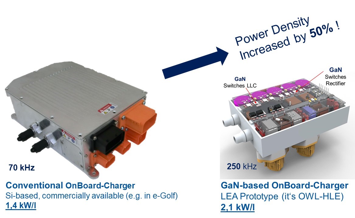
Wide Bandgap-(WGB-)based power semiconductors like Gallium-Nitride (GaN) or Silicon-Carbide (SiC) show massive innovation potential for various power electronic applications. These new semiconductor technologies characterized by significantly reduced switching losses enable both, power electronic systems with highest efficiency values and outstanding power densities, meaning a considerable miniaturization of power electronic applications. As a consequence, also the system costs of a large number of applications, like e.g. on-board chargers & DC-DC-converters of automotive EVs, IT-power supplies of data centers and mobile telecom networks (5G and beyond), renewable energy generation/transmission/distribution, medical appliances (CT, MRT, ultrasonics) can be decreased, although the WBG-semiconductor components today show higher costs than their conventional, silicon-based counterparts. Next to the component costs, the comparably rare reliability data of the new WBG-power semiconductors are considered as a last hurdle to be passed before ramping up an industrial large-scale utilization of this groundbreaking technology. This ramp up, moreover would lead to reduced WBG-component costs further accelerating the technology transition.
Project objectives
Accordingly, two main objectives will be addressed at LEA within the next years: Identification, development and optimization of further advantageous applications benefiting from WBG-based power designs as well as improving reliability of those WBG-based power electronic applications. Focusing on these topics, special support shall be offered also to small and medium-sized enterprises within dedicated follow-up projects.
The new lab infrastructure currently being acquired and put into operation in our 2-story lab building (IW) will enable LEA to adequately meet these objectives throughout the next decade.
Project strategy
The FUTURE LAB equipment enables the following technological steps as strategical subjects:
- Reducing the size of chokes, transformers and filter components by drastically increasing the switching frequency of power electronic
- Characterization of new WBG-semiconductors regarding switching behaviour and losses
- Validation of core and winding losses in magnetic components
- Professional manufacturing of custom-made mechanical components like coil formers or ferrite cores for specialized magnetics
- Extensive qualification of developed demonstrators and prototypes, incl.:
- EMI Testing and optimization
- Testing and improving operation under harsh climate conditions
- Reliability analysis of components and prototype systems under climatic stress conditions
Technological Challenges
Below challenges are considered and will be addressed by appropriate lab equipment:
- Fast switching of WBG-semiconductors leads to a high demand in EMI-filtering and -shielding
- High dv/dt-rates stress the isolation of transformers, drive circuits and auxiliary power supplies
- Novel packages of power semiconductors require special concepts for cooling and new thermal solutions
Envisaged Investments
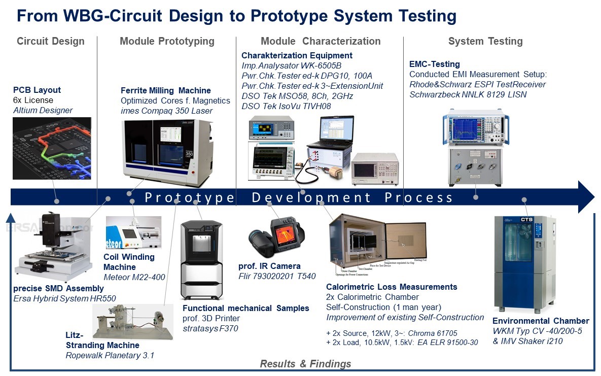
The main laboratory equipment investments are:
- Professional CAD-tool for multilayer PCB-design (SW)
- Precise assembly unit for smallest SMD-components
- 3D-printer for specifically designed mechanical components
- CNC-milling machine for application-optimized ferrite cores within magnetic components
- Coil winding machine (CNC) for magnetic components
- Testbed for high-dv/dt switching loss measurements
- Testbed for calorimetric efficiency measurements
- Testbed for EMI-measurements
- Climatic exposure test chamber with vibrating table for environmental testing
References
| [1] | C. Henkenius, N. Fröhleke and J. Böcker, „Numerical Optimization of Passive Line Filter Components for Supression of Electromagnetic Interference (EMI)“, in APEC, 2016 |
| [2] | S. Bolte, L. Wohlrab, K. Afridi, N. Fröhleke and J. Böcker, „Calorimetric Measurement of Wide-Bandgap Semiconductors Switching Losses“, in PCIM Europe, 2017 |
| [3] | S. Bolte, N. Fröhleke and J. Böcker, “GaN Buck Converter in CCM with Optimized High-Frequency Inductors”, PCIM Europe, 2018 |
| [4] | L. Keuck, N. Jabbar, F. Schafmeister and J. Böcker, “Switching Loss Characterization of Wide Band-Gap Devices by an Indirect Identification Methodology”, European Conference on Power Electronics and Applications (EPE ECCE), 2018 |
| [5] | B. Strothmann, F. Schafmeister and J. Böcker, “Pareto Design and Switching Frequencies for SiC MOSFETs Applied in an 11kW Buck Converter for EV-Charging”, 2019 IEEE Applied Power Electronics Conference and Exposition (APEC), 2019 |

